The bottleneck in research isn't ideas.
It's how fast you can hold one in your hands.

We're bridging that gap.

A post-process for standard and specialized SLA printers that replaces IPA chemical washing entirely, enabling rapid prototyping and manufacturing of high quality, biocompatible microfluidic chips, organoid housings, and applications nobody has built yet because the parts took too long to make.

IP: Patent pending License: UT System, in negotiation Origin: Sun Lab, UTSA
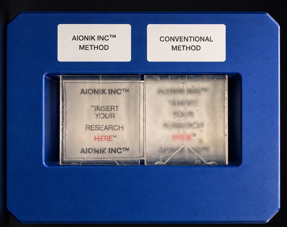
Side-by-side comparison of two microfluidic chips: the Aionik Inc. method produces an optically clear chip, while the conventional method result is hazy and distorted.

This page is long on purpose. The science is genuinely nuanced and the market case depends on details that do not compress well, so nothing has been cut. The whole argument, with its sourcing, runs about eleven minutes. Underneath it sit five deeper pages, listed at the foot of the contents below and linked from the sections they support.

Why it matters

The bottleneck

Every breakthrough starts as a concept, but concepts do not answer questions or save lives. Prototypes do. We are building the technology that turns a researcher's idea into something real in minutes instead of weeks, so the best minds in biomedical science spend less time waiting and more time discovering.

Our patent pending curing process strips away the chemicals, the solvents, and the delays that have slowed micromanufacturing for decades.

The moment

Why now

Regulators moved off animal testing, demand runs wider than biology, and all eight analyst houses have the market compounding through the next decade.

Regulators set a clock.

Capacity did not move with demand.

Microfluidic chips are still cast by hand. Soft lithography needs a cleanroom to build the mold, then, in rough order of what they cost, a mask aligner, a wafer bonder, an automated coater track, a mask exposer, a plasma system, and a spin coater, plus a vacuum desiccator, a developer bench, hot plates, a curing oven, a profilometer to check what you actually made, and the fume hood and consumables around all of it. It needs someone trained to run the whole chain. That is why the capability lives inside a small number of institutions.

The process itself is slow and operator dependent, with cure conditions that shift batch to batch. And labs prototype in PDMS while manufacturing in thermoplastic, so the device they validate is never the device they ship.

The demand runs wider than biology, and it has to scale with AI.

Regulation set the clock for organ on chip work, but it is not the only pressure. When Microsystems and Nanoengineering surveyed scholars and industry for its ten ground challenges for the field, fabrication ran through the answers. Several of the ten stall not on ideas but on access to fast, high fidelity, biocompatible microfabrication: functional organ on chip reconstruction, affordable point of care diagnostics, precision that survives the print in high performance devices, and the AI guided design to fabrication loop that only closes when iteration is cheap.

Every one of those sits on the same microfluidic and additive foundation we build for. A process that turns a standard printer into a source of clear, biocompatible parts in minutes moves the fabrication half of each problem at once. The pull is not a single market. It is a field wide shift toward tools that let a lab hold an idea in its hands the week it has it, across diagnostics, computing, and medicine alike.

Underneath all of them sits the same dependency: fabrication fast enough to prototype, cheap enough to repeat, consistent enough to automate, and able to scale without switching process. Where our process fits is the rest of this page. How we intend to commercialize it is deliberately not public, and we share that under NDA with investors and partners who need it.

The market is large, and the analysts disagree about how large.

Eight research firms publish a microfluidics market size. For nominally the same market they report figures between $9.4 billion and $41.9 billion, a spread of more than four times. That gap is about scope, whether a report counts diagnostics alone or the full device, component, and instrumentation ecosystem, rather than about growth.

Market today
$27B
Median of eight estimates, base years 2023 to 2025. Range $9.4B to $41.9B. Average $27.7B.
Forecast
$67B
Median forecast across target years 2030 to 2035. Range $21.7B to $223B. Average $84.3B, pulled up by a single outlier.
Growth
8.3 to 24%
Compound annual growth rate. Six of the eight project double digits; the lowest two are 8.3% and 8.7%. Average 12.8%.

What the eight agree on matters more than what they dispute. All of them project sustained growth, North America leading, and medical and diagnostics as the largest application. Six of the eight put compound growth in double digits, and the two lowest are 8.3 and 8.7 percent. Mordor Intelligence carves out organ on chip as the fastest growing sub technology in the field at 22.7 percent, which is the segment our biocompatible housings serve.

Growth at those rates runs straight into the constraint described above. A market cannot compound at double digits for a decade while the parts it depends on are still cast by hand in a cleanroom. That is the bottleneck, and it is the one we removed.

The eight estimates, as published

Figures as published by each firm, with no normalization across differing scope definitions. Base years differ, so these are not strictly like for like. Treat the range as an indication of scale, not as a precise market size.
The incumbent process

The current microfluidic process

Eleven steps, two days of hand work, a cleanroom for the mold, and one attempt at the bond.

Soft lithography is the standard way to make a microfluidic chip, and it has been for two decades. What it involves is the reason the capability lives inside a small number of institutions.

Eleven steps, two days

A silicon wafer is spin coated with photoresist, baked, exposed through a mask, developed, and silanized to make a mold. Only then does the PDMS get mixed, degassed, poured, cured, cut out, punched, and bonded.

Every port is made by hand

Inlet and outlet holes are punched individually into each slab with a biopsy punch. A torn port or a fragment of debris in the channel is a scrapped chip.

The bond is a deadline

Plasma activation decays within roughly 15 minutes to an hour. Alignment and contact have to happen inside that window, once, with no second attempt.

The seam is the weak point

A finished chip is two pieces held at an interface. That interface is what delaminates under pressure, and it is why these devices are treated as consumable rather than durable.

And then you wait

Two days of work does not mean a chip in two days. A lab that owns a cleanroom can turn a new design in about a week. Most labs do not own one, so the design goes out to a foundry, and the answer comes back in one to twelve weeks depending on the vendor and the complexity. Researchers routinely wait months to hold a design they drew in an afternoon, and every revision starts the wait over.

See the full process, step by step Eleven steps, the failure modes, and what the equipment actually costs.
Cost

What the current process costs

What the alternatives cost.

Overhead Per iteration Ceiling
PDMS soft lithography Cleanroom, mask aligner, trained operator Hours to days in house, weeks by foundry order Cannot scale to production
Thermoplastic injection molding Mold tooling per design Weeks, and a new mold for any change Locks the design before it is validated
Glass and silicon Semiconductor facility access Weeks Cost per chip stays high
Aionik™ Desktop printer and our unit Print runs from 20 to 30 minutes up to 1 or 2 hours depending on device size and printer, multiple chips per plate. Cure is 1 to 3 minutes Scales to production at the lowest cost per chip, same process throughout

Every existing option forces a tradeoff between speed and scale. Soft lithography iterates but cannot produce. Molding produces but cannot iterate. We hold both, in one material, with no cleanroom and no tooling.

Most labs own none of this, so they send the design out and buy finished chips. That is not a fabrication method, it is a way of paying for one, which is why it is not in the table. It removes the capital cost and replaces it with a queue: one to twelve weeks per revision, priced per order, with setup and tooling charged against every new design.

The tradeoff is also a bill. A research bench that cannot produce at volume starts at $65,000. A line that can runs $650,000 to $1.67 million in equipment, and the cleanroom the mold step needs costs $250 to $1,000 per square foot to build, depending on how fine the features are, then carries an operating cost every year it stays in service, in energy, filters, maintenance, and recertification.

Our process

One process change, four results

Resin was never the obstacle. The cure was, and removing the chemicals from it changed four things at once.

Printing finally caught up. The cure was the last obstacle.

Resin printers now resolve features small enough for microfluidics at a fraction of the cost and time. What kept those parts out of biology was never the resin, though that is where the field has spent its effort, formulating clearer and more biocompatible materials one at a time. The obstacle is the cure. We changed the process, and now get optical clarity and biocompatibility out of affordable, general purpose resins, not the specialized biocompatible formulations the field has been chasing.

01

Optical clarity

Similar quality to PDMS microfluidic chips.

02

Smooth surface

Not the rough finish of traditional polymerization.

03

Biocompatibility

Even with resins that are not biocompatible on their own.

04

1 to 3 minute cures

Depending on the print.

By removing chemicals from the curing step, our method delivers what resin printing could not before. Core method developed at UTSA — US 2026/0131529 A1, patent pending.

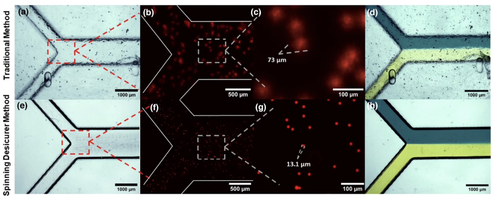
Microscopy comparison of droplet generation in the same channel geometry. Top row, traditional method: large, uneven droplets about 73 microns across with rough, blurred channel walls. Bottom row, the Aionik curing process, labeled Spinning Desicurer Method in the figure: fine, uniform droplets about 13 microns across with clean, sharply defined walls.
Same geometry, sharper result. Droplet generation in an identical flow focusing junction. The traditional method (top row) produces large, uneven droplets near 73 µm against rough, blurred walls. Our Aionik™ curing process (bottom row, labeled Spinning Desicurer Method in the source figure) produces fine, uniform droplets near 13 µm against clean, sharply defined channel walls. Figures from US 2026/0131529 A1.
The team

Why this team

Five people spanning microfluidics, materials, marketing, and finance.

Founded in San Antonio, Aionik pairs deep microfluidics and materials research with commercial and product experience.

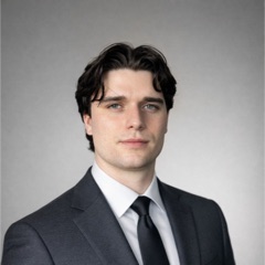
Dane Spencer

Dane Spencer

Chief Executive Officer

Finance, UTSA. Leads commercial direction from a background in financial consulting and business strategy.

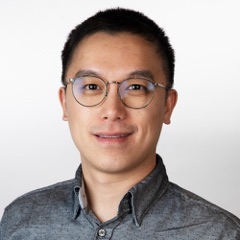
Gongchen Sun

Gongchen Sun, PhD

Chief Science Officer

Assistant Professor of Biomedical and Chemical Engineering at UTSA. PhD in chemical and biomolecular engineering from the University of Notre Dame, BS in microelectronics from Peking University. Electrokinetics, micro and nanofluidics, additive manufacturing.

Sun Lab at UTSA ↗
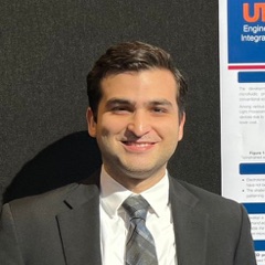
Henry Shu

Henry Shu

Chief Marketing Officer

Assistant Professor of Practice in Marketing at UTSA. Biology at UC Berkeley, an MBA at UTSA, and a Stanford Innovation and Entrepreneurship Certificate. Genomics and product marketing across biotech and diagnostics.

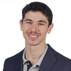
Guillermo Ramirez-Alvarado

Guillermo Ramirez-Alvarado

Chief Technology Officer

PhD in biomedical engineering, UTSA. Named inventor on the core patent application. Device architecture, process engineering, and the work of taking the curing system from a working method to a production ready design.

Gabriel Garibaldi

Gabriel Garibaldi

Director of Applied Science

Biomedical engineering, UTSA, with a PhD in chemical engineering. Named inventor on the core patent application. Materials, biocompatibility, and extending the process beyond microfluidic chips.

Evidence

What we can show

A published patent application, an exclusive license under negotiation with the UT System, and results developed at UTSA.

Intellectual property
US 2026/0131529 A1 — patent pending. Core post-processing method, filed July 2025 and published May 2026, assigned to the University of Texas System. Exclusive license to Aionik under negotiation.
Origin
Developed in the Sun Lab at UTSA. Comparative droplet generation data is shown above under The insight.
Contact

See the process for yourself

The fastest way in is a short call. Leave your details and a note, and we will reach out. We will show you what is built and answer whatever you want to ask about the process.

We follow up by email. Your details go to the Aionik team only.